Creating a simple circuit board with gschem and pcb 2007-04-14
gschem and pcb are parts of the gEDA (GPL Electronic Design Automation) suite of open source tools which can be used to design and build an electronic circuit board (amount other uses).
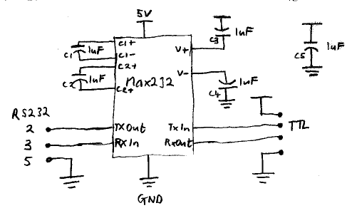
In this blog entry I'm going to design a simple serial adapter which will convert Transistor-Transistor Logic (TTL) signals into RS-232 signals. I need this adapter to be able to interface a cool little ultrasonic range finder a LV-MaxSonar-EZ1 from Maxbotix with my iPAQ.
The circuit for this adapter is very simple and only needs one chip, five capacitors and some suitable connectors or wires. With the right selection of components the full circuit can be easily housed inside a 9 pin D-shell connector.
The chip type I'm going to use is the MAX232 a Dual EIA-232 Driver/Receiver. (Note: after more research I think a MAX232A is more a useful chip type to use for this circuit.) I already have two different packaged versions of the MAX232 from Texas Instruments, a number of the MAX232IN (DIP) and of the smaller MAX232DR (SOIC). For this project I'm going to use the DIP version of the chip.
Image 1 shows a back of an envelope sketch of the circuit I'm going to create.
I'm using a version of the geda tools from CVS, but I'm not going to cover the compiling and installation of the geda tools. Use the version in your Linux distribution or checkout the geda website for more details get a suitable version.
gschem
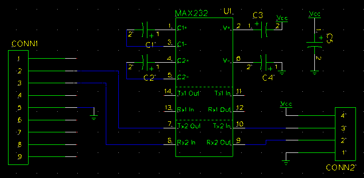
The first step is to use gschem the schematic capture program to draw out a suitable circuit diagram.

The gschem program has a fairly standard graphical user interface and operates like many graphics programs, a mouse is used to select and preform almost all the manipulation of graphic components. gschem has extensive support for keyboard shortcuts, which I'll use in this blog entry.
The first step is to add the major components. Press i key.

In the popup dialog select the "maxim", "max232-2.sym" symbol, the click on the main page to place one component. Also place one of each of the following.
- "analog", "capacitor-2.sym" symbol.
- "connector", "connector4-1.sym" symbol.
- "connector", "connector9-1.sym" symbol.
- "power", "vcc-1.sym" symbol.
- "power", "gnd-1.sym" symbol.

To zoom in on a specific area of the page place the mouse in the centre of that area and press the z key, to zoom out press the shift z keys. You can also use the scroll button on your mouse, or the menu you for more zoom options.
Lets quickly discuss the main parts of a symbol, see Image 5.
- The first main part of a symbol is made up of green lines, these are purely visible and don't effect the operation of the symbol. They are used to give the symbol shape and can also contain descriptive text about the symbol or pins.
- The next main parts are pins, they are white lines with a small red tip, there will also be an associated pin number in yellow. Pins are used to provide the the connection points between symbols, nets are used to form the links between these pins. Nets will snap to the red tips.
- The last visible part is known as the refdes and is used to uniquely identify each component in the schematic. The refdes is yellow and usually begins with a single letter and a question mark. The question mark value will be changed by the user to form a unique value.
- A symbols can also contain invisible (and visible) attributes, these attributes are used to add or change information about the symbol.

The next step for me is is set some of the attributes of the placed components. To select a component just click on it, it will then turn a brown colour. See Image 6.

Once a component is selected, you click and hold the mouse button down to move the component to a different location. When a component is selected if you press the e key and then the e key again or double click on the component, it will bring up the components edit attribute dialog.

In this dialog we can add new or edit existing attributes.
- For the capacitor symbol edit the refdes value to "C1" and add an attribute named "footprint" with the value "RCY100P" (make it invisible).
- For the MAX232 the refdes value is "U1" and the footprint is "DIP16".
- For the 9 pin connector the refdes is "CONN1" and the footprint is "SIP9".
- For the 4 pin connector the refdes is "CONN2" and the footprint is "SIP4".
- The Vcc and GND symbol doesn't need any attributes.
The circuit requires five capacitors, so we could add four more capacitor symbols and edit all the attributes on each, but it is quicker to copy the existing capacitor. Select the capacitor and press the e key and then the c key. Now place the copied symbol somewhere on the page, all the attributes have be copied, we just need to change refdes attribute to C2. And repeat until we have five capacitors C1 to C5.

Lets quickly cover nets. A net provides a link between one or more pins, you can think of it as a piece of wire, but in a circuit board it is more likely to be a copper trace. You can start a net by pressing the n key, using the menu or toolbar button.
An unconnected net has a small red square at the ends. A join between two nets has a small red circle. With a join between a pin and net having no red square or circle. You should be aiming to have no unconnected nets in your schematics.

Image 9 show seven examples of nets, from left to right and top to bottom.
- A single unconnected net.
- A single unconnected net with two 90 degree bends.
- A two crossing unconnected nets.
- A two crossing nets joined at a centre point.
- A complex example with five unconnected nets joined at three points.
- A net connect to only one pin.
- A net forming a connection between two pins.
The next step is to move the components around and link them together with nets. Move the components by selecting and dragging them to the correct location. A component can be rotated 90 degrees by pressing the e key and then the r key.
A useful feature is that pins can be joined together without a net just by placing the red tips together.
Also Vcc and GND have pins have named nets, any named nets which share the same name are automatically linked together. This means we don't have to place extra nets to join all the Vcc and GND points, helping to keep the schematic clean and clear.
One other item to note is that the MAX232 symbol doesn't have a visible Vcc and GND pin, the symbol contains invisible named nets which provide these links. This type of symbol design isn't in common use now and explicit visible power pins are recommend in all new symbols.
Next time I will cover converting this schematic into a circuit board using pcb.